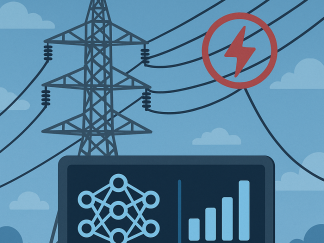


Understanding SRAM Design Landscape: Circuits and Materials-Based Perspective
Join this comprehensive webinar exploring cutting-edge SRAM design methodologies, from circuit-level optimization to advanced materials integration, led by renowned VLSI expert Dr. Ashish Sachdeva.
Register Now - FreeAbout This Webinar
This webinar provides an in-depth exploration of SRAM (Static Random Access Memory) design from both circuit-level and materials perspectives, covering advanced techniques for stability improvement, power reduction, and performance optimization in modern semiconductor technologies.
Research Excellence
Dr. Sachdeva's research encompasses comprehensive SRAM design innovations, spanning from fundamental circuit architectures to advanced materials implementation, with significant contributions to stability analysis and low-power design methodologies.
Research Impact
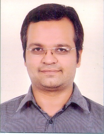
Featured Speaker
Webinar Curriculum
A comprehensive journey through SRAM design principles, from foundational concepts to cutting-edge research in circuit optimization and materials science
Overview of SRAM architecture | Comparison with DRAM and other memory technologies | Key performance metrics (read/write stability, speed, power) | Evolution of SRAM design across technology nodes.
Structure and operation principles | Read and write mechanisms | Stability analysis using butterfly curves | Limitations and challenges in scaled technologies | Static Noise Margin (SNM) analysis.
8T, 10T, and beyond: architectural innovations | Improved read stability techniques | Write-assist mechanisms | Performance comparisons and trade-offs | Application-specific cell selection criteria.
Supply voltage scaling strategies | Subthreshold SRAM operation | Power gating and retention techniques | Dynamic voltage and frequency scaling | Energy-efficiency optimization methods.
Process variation impacts on stability | Read stability improvement techniques | Write margin enhancement strategies | Half-select disturbance mitigation | Statistical design approaches.
FinFET technology for SRAM | FDSOI advantages in memory design | 2D materials (graphene, TMDs) integration | Emerging device technologies (TFETs, NCFETs) | Material selection impact on performance.
Short-channel effects in scaled SRAM | Process variation and mismatch | Soft error susceptibility | Leakage current management | Temperature and voltage variation effects.
IoT and ultra-low-power requirements | Near-threshold computing | In-memory computing architectures | AI/ML accelerator memory | Automotive and safety-critical applications.
SPICE-based circuit simulation | Monte Carlo variation analysis | Corner analysis techniques | Power estimation tools | Layout considerations and DRC/LVS.
3D-stacked memory architectures | Spin-transfer torque MRAM integration | Neuromorphic computing memory | Quantum-dot cellular automata | Research opportunities and career guidance.
Frequently Asked Questions
Contact & Support
For queries regarding registration, participation, or technical issues, please email:
ieee.mtts@iiitm.ac.in
Or call: +91-9876543210
Ready to Join the SRAM Design Webinar?
Reserve your spot now and gain insights from leading experts in VLSI and memory design. Registration is free and open to all interested participants.
Register Now - Free